For the Semiconductor Switch
Device Research page, click Here.
My primary area of
interest is the
simulation of high electric field transport in photoconductive
semiconductor switch (PCSS)
materials such as GaAs. This
is where my
funding
(Sandia National
Laboratories
& the Air Force Office of Scientific Research, AFOSR)
comes from.
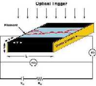
A schematic of a PCSS is shown here:
High field transport
simulations in PCSS
materials were the dissertation topics of my last two PhD students,
Samsoo (Sam) Kang(PhD, 1998)
& Kenneth (Ken)Kambour(PhD,
2003).
At Sandia,
my collaborator is Harry
Hjalmarson, who served as
co-Advisor to Ken Kambour. Ken
is now a post-doc at Sandia, working on
some extensions of his dissertation work. There, he can interact
directly with Harry Hjalmarson, as
well as with our experimental collaborators (Fred
Zutavern&
co-workers).
Sam Kang's dissertation was a "proof in principle"
that the
collective impact ionization theory of Hjalmarson,et
al.
is correct. The basic idea of this theory is that, at high
electric
fields AND high
carrier densities, carrier-carrier (cc) scattering enhances the impact
ionization rate, thus leading to electrical breakdown at fields much
lower than the usual
breakdown field. Using an Ensemble Monte Carlo
(EMC) approach to high field transport,
Sam successfully applied this theory to GaAs.
In Ken Kambour's dissertation, a collective impact
ionization
approach was used to develop a generalized theory of electrical
breakdown in insulators, which includes the dependence of impact
ionization on both the electric field and the carrier density. This
theory was applied to PCSS materials and was
used to explain the lock-on effect, an optically-triggered breakdown
that occurs in GaAs and InPPCSS's.
This generalized breakdown
theory uses a rate equation approach to find
the carrier densities which, at a given electric field, result in a
steady state. In this approach, the competition between carrier
generation (by impact ionization) and carrier
recombination (by Auger
and defect recombination) governs whether or not electrical
breakdown
occurs. This leads to a definition of the bulk breakdown field as the
lowest field for which the injection of an infinitesimally small
carrier density will result in a steady state with a large carrier
density. It also leads to the definition of the lock-on field as the
lowest field for which a stable, non-zero steady state carrier density
is possible.
To implement this theory, the EM
method was
used to calculate the carrier distribution function, including the
effects of carrier-carrier scattering. Since the EMC calculations are
computationally intense, this implementation also used both low and
high density approximations for the distribution function. The low
density limit was obtained using the EMC method without the inclusion
of cc-scattering.
The high density limit was obtained
by approximating the distribution function as a Maxwellian. Using this
theory, predictions were made for both the lock-on field and the bulk
breakdown field in GaAs, InP, Si,
and GaP.
In this theory, the lock-on effect is a type of
carrier-density
dependent electrical breakdown which occurs in all insulating
materials. Further, it is the difference between the predicted lock-on
and breakdown fields which determines whether or not the lock-on effect
will be observable as a phenomenon distinct from ordinary breakdown.
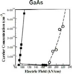
Typical results are shown in the figure below, which
plots
the
predicted steady state carrier density as a function of electric field
for GaAs.
The hollow circles are the EMC results without
carrier-carrier scattering. The solid circles are the EMC results with cc-scattering. The squares are Maxwellian results. The curves
are
included to guide
the eye. The predicted breakdown field is the field (~177 kV/cm)
at
which the dashed curve intersects the horizontal axis. The predicted
lock-on field is the minimum field (~90 kV/cm)
on
the solid
curve.
Predicted Steady State
Carrier Density vs. Electric Field for GaAs
Recent publications which resulted from this project are #2,3,13,17 & 18
on the "Recent
Publications" link below.
This project has
also resulted in MANYconference presentations.
See #1,2,7,16,19,22,25,28,32,34
& 35
on the "Recent
Conference Presentations" link below.
Ken
Kambour's dissertation: Abstract
(Word); Document
(PDF, 2.84 MB, 102 pages). PhD Graduation Photos.
Recently, through collaboration
and
consultation on the MURI
Compact Pulsed Power Program, a small effort on semiconductor
switch
device simulation has been started. More details on this topic may be
found Here.
Abstract
for a recent colloquium
on semiconductor switches. (Word, 89.5 kB) Slide
summarizing recent work on the Sandia project. (Power
Point, 187 kB).